
Meta description (140–160): Visualize nanostructures with NANOTEC’s E-SEM—up to 300,000× magnification for morphology and particle size, with ISO/IEC 17025 accreditation for sizing in the 100–1,000 nm range.
SEO Keywords: e-sem thailand, environmental scanning electron microscope, morphology analysis nanoparticles, particle size from images, iso iec 17025 100–1000 nm, nonconductive sample imaging, materials characterization thailand, cosmetics materials testing, electronics failure analysis, sem services thailand
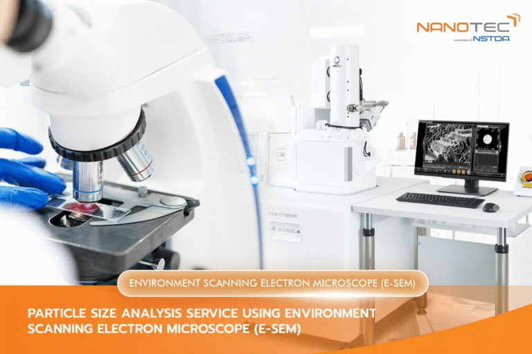
Why E-SEM Matters
Surface structure tells the story behind performance. In cosmetics, it influences feel, spreadability, and light scatter. In polymers, coatings, textiles, electronics, and powders, it governs adhesion, durability, flow, and reliability. Optical microscopes often can’t resolve features below a few hundred nanometers—and sample prep (coating, dehydration) can distort delicate materials. The Environment Scanning Electron Microscope (E-SEM) addresses these constraints by enabling high-resolution imaging at up to 300,000× magnification, with operating modes that accommodate non-conductive or more hydrated specimens better than conventional high-vacuum SEM. You see real features, not artifacts—so you can connect microstructure to product behavior with confidence.
What E-SEM Delivers
E-SEM provides crisp, high-contrast images of surface morphology and permits particle size assessment from images where appropriate. Typical uses include:
- Nanoparticle agglomeration & shape—distinguish primary particles vs. agglomerates; evaluate dispersion quality.
- Coating integrity—inspect cracks, pores, and layer uniformity across films and treated surfaces.
- Powders and fillers—examine particle edges, porosity, and secondary structures that affect flow and packing.
- Textiles and fibers—visualize fibrillation, cross-sections, and surface treatments that influence comfort and performance.
- Electronics and printed features—inspect feature edges, defects, and residues on non-conductive substrates.
Because E-SEM relaxes strict high-vacuum requirements, many samples need minimal or no conductive coating, reducing the risk of altering the very surfaces you wish to study.
Accredited Range & Reporting You Can Trust
For projects where specifications and audits matter, NANOTEC offers ISO/IEC 17025 accreditation for particle sizing in E-SEM images across 100–1,000 nm. That means our measurement workflow—imaging conditions, calibration, and image-analysis routines—has been validated for that size window.
Your report can include:
- Representative micrographs with scale bars and magnification.
- Particle size statistics (within the accredited 100–1,000 nm window, when image-based sizing is applicable).
- Method notes: operating mode, accelerating conditions, working distance, detectors used, calibration references.
Note: Image-based sizing reflects 2D measurements of visible particles/edges in fields of view. For colloids in liquid, combine with DLS for hydrodynamic diameter and distribution; for ultra-fine internal structure, consider TEM.
When to Choose E-SEM vs. Other Methods
- Choose E-SEM for morphology (edges, pores, cracks), to verify particle shape/agglomeration, to illustrate defects, or to measure particles within the 100–1,000 nm accredited window directly from images.
- Choose DLS for fast, in-liquid size distributions and zeta potential on dispersed systems.
- Choose FE-SEM/TEM for ultra-high magnification or internal structure beyond E-SEM’s limits.
- Add AFM/Contact Angle/BET when roughness, wettability, or powder surface area drive performance.
Together these techniques yield a coherent dataset—visual proof plus quantitative metrics—fit for QA, regulatory, and customer documentation.
Sample Guidance (What to Prepare)
- Clean, representative pieces large enough to mount; mark target areas (coated side, fracture edge, print feature).
- Avoid loose dust, oils, fingerprints on regions of interest.
- For powders, supply dry material in a sealed container; note if dispersion or pressing is preferred.
- Share sensitive conditions (heat, vacuum, solvents) so we can select suitable E-SEM parameters.
E-SEM’s variable-pressure modes can mitigate charging on insulating samples, often avoiding heavy metal coatings that obscure features.
Who This Service Is For
- Corporate & OEM/ODM (Coatings, Polymers, Cosmetics, Electronics).
You need audit-ready morphology and, where applicable, accredited particle sizing (100–1,000 nm) to support specifications, vendor control, and customer reports. - SMEs.
You want clear pictures and straightforward explanations that drive decisions—whether to change a supplier, tweak a process, or set realistic tolerances. - Universities & Research Institutes.
You’re validating treatments or structures at the nanoscale and need publication-friendly micrographs plus size statistics where relevant. - Tech Startups.
You need visual proof for investors or partners. Use E-SEM images to demonstrate differentiation (smoother coatings, tighter particles) before moving to more costly studies. - Overseas Customers/Investors.
You require standardized reporting and recognized ISO/IEC 17025 accreditation ranges suitable for cross-border stakeholders.
Pricing Overview
Scope your session with the guide below; we’ll confirm a formal quote based on sample type, number of regions, and any replicated measurements.
- E-SEM morphology / particle sizing (image-based): from THB 500 per item
- Add-ons: multiple fields of view, additional regions, repeatability sets, annotated image packs, combined E-SEM + DLS/TEM bundles
Frequently Asked Questions (recap)
What magnification is available? Up to 300,000×.
Is particle sizing accredited? Yes—ISO/IEC 17025 for 100–1,000 nm (image-based, where applicable).
Do you need to coat samples? Often no or minimal coating thanks to environmental modes.
What if my material is a liquid dispersion? Use E-SEM for dried/mounted specimens and DLS for in-liquid sizing.
Can you compare suppliers or batches? Yes—side-by-side imaging and metrics are available.
Suggested Internal Links (provisional; finalize later)
- Testing & Analysis Hub
- DLS — Particle Size & Zeta Potential
- AFM — Nanoscale Surface Topography
- TEM — Internal Nanostructure (Imaging)
- Chemical Analysis — FTIR / Raman / GC-MS / LC-MS/MS
Call to Action
Book an E-SEM session or request a quote for morphology and accredited particle-size analysis. We’ll help you select fields of view and complementary methods to build a decision-ready dataset.
Infrastructure Services
National Nanotechnology Center (NANOTEC)
143 INC 2 (B), Thailand Science Park, Phahonyothin Road, Khlong Nueng, Khlong Luang, Pathum Thani 12120
Tel. +66 2 564 7100 ext. 6517, 6625, 6680
Email: bdis-infs@nanotec.or.th