
Meta description (140–160): Characterize surfaces at the nanometer scale with NANOTEC’s AFM—topography, mechanical and electrical property mapping—backed by ISO/IEC 17025 certification for size measurements in the 100–1,000 nm range.
SEO Keywords (one line): atomic force microscopy afm thailand, nanoscale surface topography, iso iec 17025 afm 100–1000 nm, surface roughness nanometer, nanomechanical mapping, electrical property mapping, coatings films polymers, biomaterials cosmetics testing, electronics surface characterization, materials characterization thailand
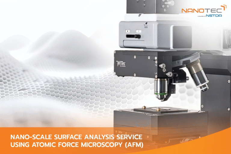
Why AFM at NANOTEC Changes the Game
Surface performance is decided in the first few nanometers. Adhesion, gloss, printability, tactile feel, biocompatibility, even electrical reliability—all trace back to nanoscale texture and near-surface properties. Yet these are the details teams most often guess at: optical tools can’t resolve them, and conventional SEM shows morphology without true height data. That gap leads to fragile specs, supplier disputes, and costly rework when coating lines or formulations scale.
The National Nanotechnology Center (NANOTEC) closes this gap with Atomic Force Microscopy (AFM) services that turn nanoscale uncertainty into evidence. We scan surfaces to produce true 3D topography and roughness metrics, with optional mechanical and electrical contrast mapping—so you can connect process changes to measurable outcomes. Work is delivered within an ISO 9001 quality system, and AFM is ISO/IEC 17025 certified for size measurements in the 100–1,000 nm range, giving QA and partners confidence in your data.
Because AFM sits inside NANOTEC’s broader testing ecosystem (e.g., E-SEM for morphology, NMT for indentation/scratch/wear, Contact Angle for surface energy, BET for powders), you can build a coherent, cross-method dataset when decisions require it—without juggling vendors. The result: specifications you can defend, faster troubleshooting, and a clearer path from R&D to production.
What AFM Measures: Topography, Mechanical, Electrical
AFM is a versatile platform. Depending on operating mode and probe, it can deliver:
- Topography & roughness. Quantitative height images, line profiles, Ra/Rq/Sa parameters, feature dimensions, pattern fidelity.
- Mechanical property indicators. Force–distance/phase-contrast signals related to relative stiffness/modulus, adhesion, and viscoelastic response at or near the surface (mode-dependent).
- Electrical property indicators. Selected modes enable qualitative mapping of near-surface electrical behavior (e.g., charge distribution), useful for patterned films or treated surfaces.
Use AFM when you need nanoscale surface evidence: verifying coating uniformity, comparing treatments, detecting nano-defects, or quantifying texture that drives adhesion, printability, comfort, or optical appearance.
Accredited Size Range & Reporting
For projects where specs and audits matter, NANOTEC’s AFM service is ISO/IEC 17025 certified for size measurements in the 100–1,000 nm range. This accreditation covers our measurement workflow—instrument calibration, image scaling, and analysis routines—within that window.
Your report can include:
- Height/topography images with scale bars and selected roughness statistics
- Line profiles and feature dimensions (within the certified range where applicable)
- Mode notes & conditions: probe type, scan size, resolution, setpoints, filters/flattening steps
- Optional overlays/contrast for mechanical or electrical mapping (qualitative, mode-dependent)
Typical Deliverables
Most clients request a concise, decision-ready package:
- Topography images (1–3 representative areas) with roughness metrics
- Profiles/measurements of key features (e.g., particle or pattern height, spacing)
- Interpretive notes connecting observed texture/defects to likely performance implications
- Optional property maps (mechanical/electrical indicators) for comparative studies
Sample Guidance (How to Get Reliable Images)
Accurate AFM starts with surfaces prepared to reveal true features—not artifacts.
- Provide flat, clean, representative areas; avoid fingerprints, dust, loose fibers.
- Indicate areas of interest (coated side, patterned region, scratch/wear track).
- For soft/tacky samples, note temperature or conditioning needs; we’ll select gentle scan parameters.
- For powders or particles, discuss mounting/immobilization (pressed film, adhesive substrate, drop-cast) to prevent probe drag.
- Share any treatments/cure schedules so we can interpret mechanical contrast correctly.
When to Choose AFM vs. Other Methods
- Choose AFM for nanoscale topography and near-surface property contrast where optical or SEM methods cannot resolve height quantitatively.
- Choose E-SEM/FE-SEM when you need wider field morphological context, high-contrast imaging, or elemental analysis (EDX).
- Choose NMT (nano-mechanical tester) for standardized indent/scratch/wear at controlled loads across larger areas.
- Add Contact Angle/BET when wettability or powder surface area/porosity also drive performance.
- Pair with DLS if your film/coating originates from a dispersion and you need in-liquid particle size for process linkage.
Who This Service Is For
- Coatings, Films & Polymers (Corporate & OEM/ODM).
Quantify roughness, layer uniformity, and nano-defects to set specs, compare suppliers, and verify process changes. - Electronics, Printed Features & Thin-Film Devices.
Assess nanoscale texture and local property contrast on insulating or delicate substrates that are challenging for electron microscopy alone. - Cosmetics, Biomaterials & Medical Surfaces.
Relate tactile feel, adhesion, and optical appearance to measurable nanometer-scale texture; compare treatment or formulation effects. - SMEs & Startups (Materials, Functional Inks).
Get decisive nanoscale evidence before scaling: validate pattern fidelity, surface prep quality, or coating smoothness.
Pricing Overview
Use the guide price to scope your work; we’ll finalize a quotation based on scan areas, resolution, and any property mapping.
- AFM surface analysis: from THB 2,000 per item
- Add-ons: multi-area mapping, higher-resolution scans, mechanical/electrical contrast maps, side-by-side comparisons, annotated image packs
- Bundles: AFM + E-SEM (morphology), AFM + NMT (mechanical durability), AFM + Contact Angle (wettability link)
Frequently Asked Questions (recap)
What can AFM quantify?
Nanometer-scale topography/roughness and feature dimensions; mechanical/electrical indicators are available (mode-dependent, generally qualitative).
What is the accredited range?
ISO/IEC 17025 certified 100–1,000 nm for size measurements (within the validated workflow).
What industries do you support?
Textiles, plastics, food, pharmaceuticals, cosmetics, and electrical/electronic sectors, among others.
How should I prepare samples?
Provide flat, clean areas; mark regions of interest; disclose treatments and any sensitivity (heat, solvents).
Can AFM replace SEM?
They’re complementary: AFM adds true height data and near-surface property contrast; SEM provides wider-field morphology and elemental options (via EDX).
Suggested Internal Links (provisional; finalize later)
- Testing & Analysis Hub
- E-SEM — Morphology & Image-Based Sizing
- Nano-Mechanical Tester (Indent/Scratch/Wear)
- Contact Angle & Surface Energy
- Chemical Analysis — FTIR / Raman
Call to Action
Book an AFM session or request a quote for nanoscale surface topography with optional mechanical/electrical mapping. We’ll help you select scan areas and parameters to deliver clear, decision-ready data.
Infrastructure Services
National Nanotechnology Center (NANOTEC)
143 INC 2 (B), Thailand Science Park, Phahonyothin Road, Khlong Nueng, Khlong Luang, Pathum Thani 12120
Tel. +66 2 564 7100 ext. 6517, 6625, 6680
Email: bdis-infs@nanotec.or.th