
Graphene quantum dots split Cooper pairs
Superconducting “Cooper pairs” of electrons have been split to create entangled pairs of electrons in a new device built by physicists in Finland and Russia
Superconducting “Cooper pairs” of electrons have been split to create entangled pairs of electrons in a new device built by physicists in Finland and Russia

Fractal patterns that arise when healthy human cells turn cancerous have been observed for the first time by scientists in the US. Using an atomic force microscope (AFM), Igor Sokolov and colleagues at Tufts University and Clarkson University saw the patterns while studying the surfaces of cervical epithelial cells at nanometre resolution. The work could […]
Hot spots can occur in devices made from carbon nanotube arrays, according to new experiments by researchers at IBM in the US and Brazil and Northwestern University. The highly localized thermal centres, which can be much hotter than 400 K, can irreversibly degrade device performance and so need to be better controlled….. http://nanotechweb.org/cws/article/tech/60497 Hot spots in […]
A new “bullseye”-shaped grating has allowed researchers to efficiently collect photons with specific spins from the diamond nitrogen-vacancy (NV) colour centre. The number of photons collected reached nearly three million per second, which is the highest ever value reported to date for a single NV. The result could have important implications for a number of […]
The notion that surface structure may affect friction and adhesion between interfaces is not new. But until recently there had been no experiments with nanoparticles to test this relationship. Now researchers in Korea have made gold nanoparticles of different shapes to identify how atomic packing density at the surface affects their tribological properties….. http://nanotechweb.org/cws/article/tech/60516 Friction […]
Surface enhanced Raman scattering (SERS) is able to identify molecules at very low concentrations and so can be put to good use in many analytical applications, such as forensics, medical diagnostics and identifying new drugs. However, the technique suffers from continuous background photoluminescence, the origin of which is still poorly understood. This background makes it […]
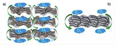
A nitrogen-doped nanocomposite made from carbon nanotubes and graphene could make an efficient and inexpensive catalyst
Correcting quantum errors in superconducting circuits Quantum computers of the future will be built from large numbers of quantum bits (or qubits), which will be in certain quantum states. However, such states are extremely fragile and are easily destroyed by “bit errors” coming from external noise in the environment, and physicists have yet been unable […]
Researchers at the University of Texas say they have made the first flexible ambipolar field-effect transistor based on few-layer black phosphorus (or phosphorene). The device has a high carrier mobility of around 310 cm2/V.s and an effective drain current modulation of more than 103. These values are better than those seen in flexible transistors made from […]


Gold nanotubes could be used to photothermally destroy cancer cells according to new experiments by researchers at the University of Leeds in the UK.
Applying circularly polarized light to a monolayer of graphene dramatically changes how surface electromagnetic waves (or plasmons) disperse along the carbon sheet. This new result, from researchers in Sweden and The Netherlands, could not only be important for studying how charge carriers move in graphene, but could also help build graphene-based elements for the rapidly […]
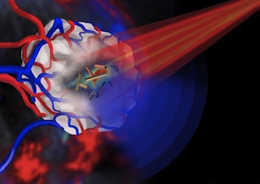
Researchers in the UK, France and the US have made the first quantum “rattles” from gold quantum dots inside a porous silica shell. The nanostructures can be heated up using light and so be used to kill tumour cells in a technique called photothermal therapy. They can also carry drugs thanks to their hollow cores, […]
Researchers in Germany and Sweden are saying that they can improve the quality of printed graphene inks using a technique called laser annealing. The method might be used to improve inks made from other 2D materials too, and so might become a standard procedure for producing such films. The graphene inks, which are transparent and […]


While carbon nanotubes (CNTs) have long attracted interest for nanoscale electronics, practical deployment of the technology requires a level of device consistency that is still a long way from being achieved
Researchers at the universities of Manchester and Sheffield in the UK have fabricated a new type of light-emitting diode by stacking up several 2D materials: metallic graphene, insulating hexagonal boron nitride and various semiconducting monolayers made from transition metal dichalcogenides (TMDCs). The devices emit light across their whole surface and have a high quantum efficiency […]
An interlocked DNA ring structure (known as a “catenane”) can be switched between two catalytic states by an external trigger – something that is not possible for a linear DNA arrangement. This result, from researchers at the Center for Nanoscience and Nanotechnology at the Hebrew University of Jerusalem in Israel, might one day be used […]
Researchers in Moldova and Germany are reporting on a new and simple way to cover the surfaces of porous semiconductors with a monolayer of gold nanodots using a pulsed electroplating technique. The method might be used to make plasmonic photonic crystals, optoelectronic on-chip interconnects and chemical and biological sensors….. http://nanotechweb.org/cws/article/tech/60254