Ban Pong Sugar visit
Representatives from Ban Pong Sugar Co.,Ltd paid a visit to NANOTEC with an aim to explore ways to utlizie waste from sugar production process eg. sugarcane fiber and left over wax on Oct 1.
Representatives from Ban Pong Sugar Co.,Ltd paid a visit to NANOTEC with an aim to explore ways to utlizie waste from sugar production process eg. sugarcane fiber and left over wax on Oct 1.
Dr. Banja and senior management of Innovation Group took this opportunity to visit NANOTEC Functional Nanomaterials and Interfaces Lab (FNI).
Dr. Banja Junhasavasdikul, CEO of Innovation Group Thailand was in NSTDA to give a talk at the CEO Talk session.
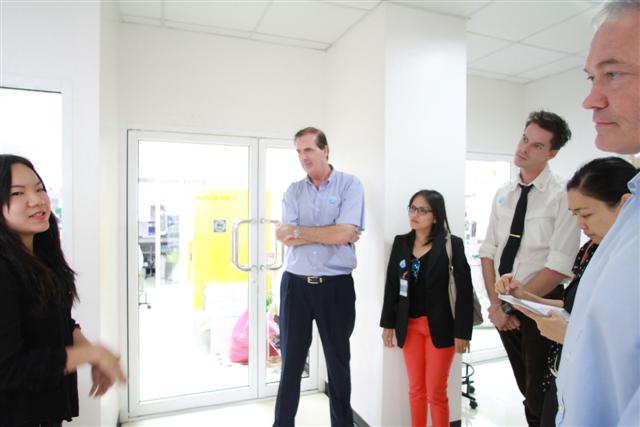
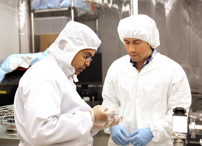
Senior management from AVEREAN International Co.,Ltd and Nina Heyer Ltd led by Mr. Theo Vera and Mr. Tim Wells visited Nano Cosmeceuitcal Lab on Sept 25
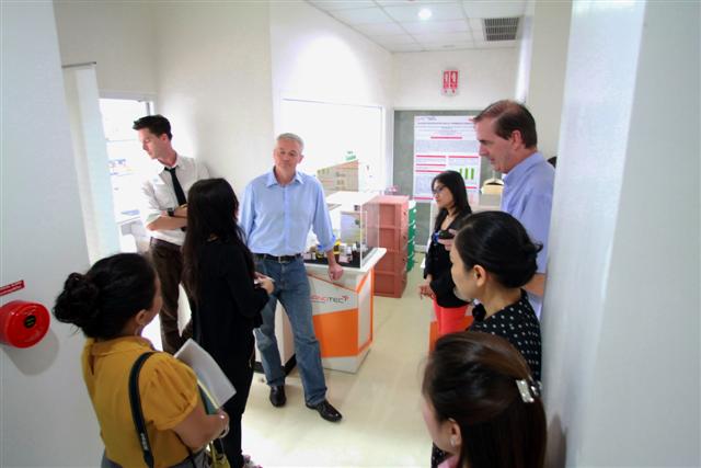
Senior management from AVEREAN International Co.,Ltd and Nina Heyer Ltd led by Mr. Theo Vera and Mr. Tim Wells visited Nano Cosmeceuitcal Lab this afternoon.
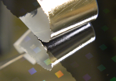
Using a technique known as atomic layer deposition and, surprisingly, a roll of sticky tape, researchers from the US and Korea have come up with a new technique to produce extremely thin gaps in metal layers.
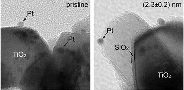
A sinter-resistant, tri-phasic catalyst made of platinum (Pt), titanium dioxide (TiO2), and silica (SiO2) has been developed by researchers at Georgia Institute of Technology in the US.
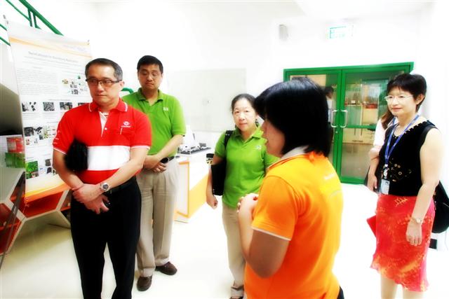
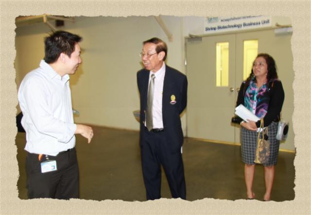
Senior management of Green Spot Co.,Ltd consisting of Mr. Thammasak Jittimaporn, CEO, Mr. Supadej Chirasavinuprapand, General Manager – Manufacturing, Ms. Aree Naratippakorn, Division Manager , R&D, and Ms. Jarunart Nongmak, Research & Development Specialist, R&D visited Nano Delivery System Lab (NDS) and Nano Characterization Lab (NCL) on September 24.
Senior management of Green Spot Co.,Ltd consisting of Mr. Thammasak Jittimaporn, CEO,

Minister visit to EMPA on Sept 15 to observe nanotechnology to improve function of fabric
The OECD has recommended its Member Countries apply existing international and national chemical regulatory frameworks to manage the risks associated with manufactured nanomaterials……

A DNA chip consists of a few hundred to ten thousand types of DNA fragments which are densely placed on a glass or resin substrate.
Representative from Toshiba R&D Center in Tokyo presented New Types of DNA Chip at NANO Talk session on Sept 19, 2013

The MOU for the 4th and final NANO Plus (TTN Network Center) was signed this morning between NANOTEC and Prince of Songkla University (PSU) at NANOTEC.
Member of the Committee on Government Organization visited NSTDA at Thailand Science Park.
Members of the Committte on Government Organization led by MP Chen Thaugsuban visited NSTDA to gain better understanding of research undertakings at NSTDA on September 18
Researchers at the University of Alberta in Canada are the first to have succeeded in synthesising colloidal zinc phosphide (Zn3P2) semiconducting nanocrystals
A new, low-cost, state-of-the-art CMOS compatible process to make flexible and semi-transparent silicon-based circuits has been unveiled by researchers at the King Abdullah University of Science and Technology (KAUST) in Saudi Arabia
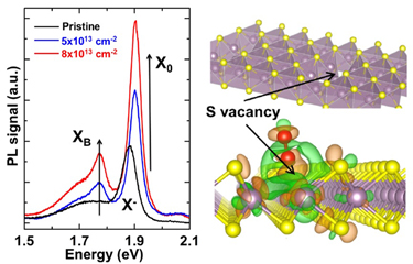
Defects are generally thought to degrade a material’s physical properties, but new experiments by researchers in the US and China have revealed that they can actually help certain 2D semiconductors

Thailand’s investment in infrastructure to support R&D: The Thailand Science Park

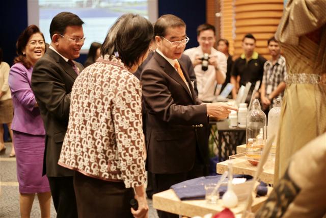
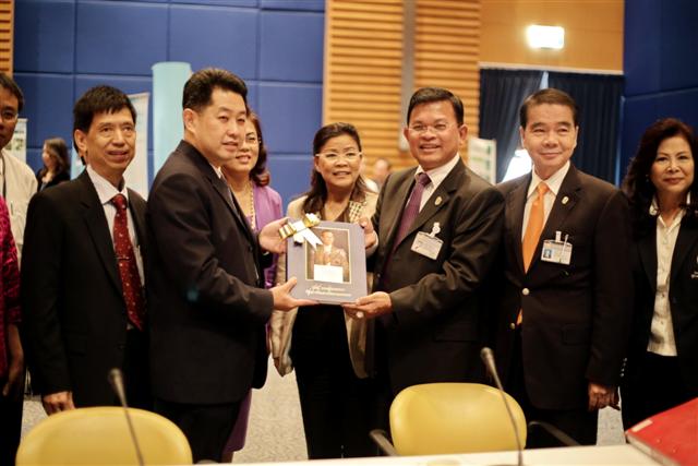
Dr. Sirirurg Songsivilai, Director of NANOTEC (Thailand’s Nanotechnology Center) spoke at the plenary session of SAICM (Strategic Approach to International Chemical Management) about nanosafety and nano ethics in Thailand at the 3rd ICCM (International Conference on Chemical Management) on 18 September 2012 in Nairobi, Kenya.