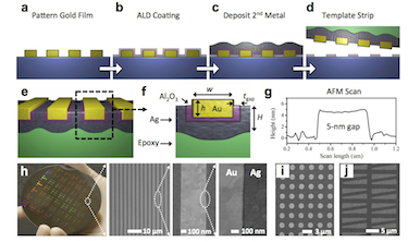
Using a technique called atomic layer lithography, researchers in the US and Italy have succeeded in creating nanometre-wide gaps in metal films. Such gaps are normally made by etching or milling a narrow strip of metal in the film, but it is difficult to make gaps smaller than 10 nm across in this way. The gaps, which resonate at certain “plasmonic” frequencies, can strongly couple to light and could be used to detect biomolecules using spectroscopy techniques like SERS (surface-enhanced Raman scattering) and SEIRA (surface-enhanced infrared absorption)…..
http://nanotechweb.org/cws/article/tech/59552
